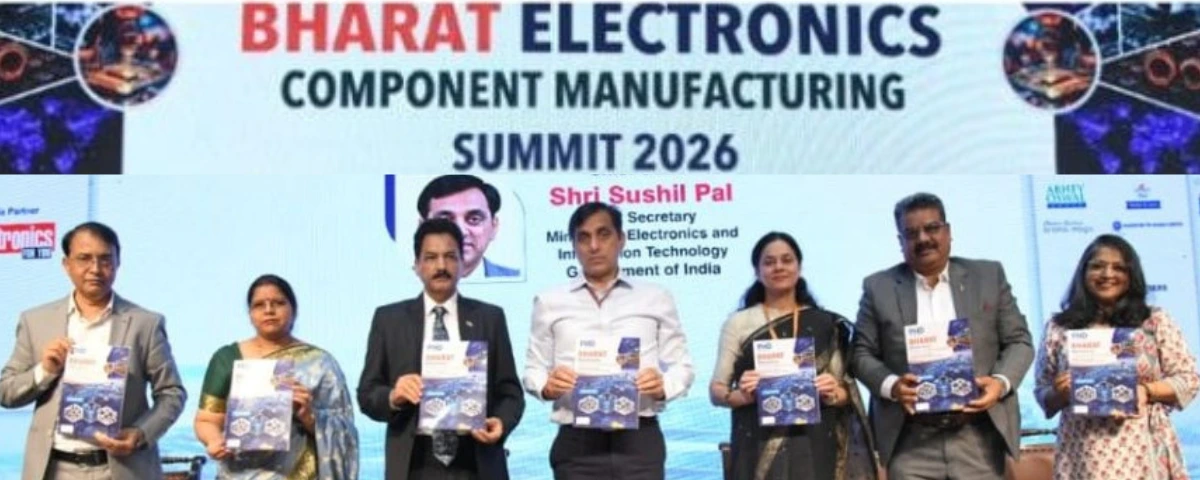
India needs to deepen its semiconductor ecosystem across components, materials, chemicals, equipment and advanced packaging as it works towards its broader electronics manufacturing ambitions, Sushil Pal, Joint Secretary, Ministry of Electronics and Information Technology (MeitY), said at the Bharat Electronics Component Manufacturing Summit 2026 in New Delhi on August 19.
Addressing the summit, Pal said India’s electronics manufacturing journey has moved from assembly-led manufacturing to sub-assemblies and modules and is now moving deeper into components, materials and the wider semiconductor supply chain.
“Finished goods can only take us so far” in achieving the country’s electronics manufacturing ambition, Pal said, stressing that a sophisticated component ecosystem would be critical to reaching the government’s target.
According to Pal, the Indian government is pursuing separate policy approaches for semiconductor and non-semiconductor manufacturing sectors. The proposed Semicon 2.0 framework is expected to extend beyond semiconductor fabrication and ATMP/OSAT facilities to components, materials, gases, chemicals, capital equipment and sub-assemblies required across the semiconductor ecosystem.
According to Pal, semiconductor manufacturing requires substantially higher capital expenditure and much higher purity standards for materials and chemicals compared with conventional electronics manufacturing.
“Semicon 2.0 does not only cover fabrication or ATMP or OSAT, but also all the components, materials, gases and chemicals which will go into making these semiconductor plants, as well as capital equipment and sub-assemblies,” Pal said.
The Indian government has so far approved 12 semiconductor proposals, which are expected to generate demand across the wider ecosystem, including substrates, lead frames, bonding materials and specialty chemicals. Pal stressed the need to develop domestic capabilities in semiconductor packaging and advanced packaging, alongside electronic-grade chemicals and other high-purity inputs.
Beyond manufacturing capacity, Pal highlighted the need to strengthen India’s technological capabilities, intellectual property and chip-design ownership. He said the government has approved 24 applications under the Design Linked Incentive (DLI) scheme, with several chip designs already taped out and expected to move towards product qualification and commercialization.
Greater investment in R&D, engineering talent and product development will be necessary to connect India’s design capabilities with its growing manufacturing base, Pal said.
He also urged companies to focus on global quality standards, saying the objective should not simply be to manufacture products in India, but to manufacture them at the right quality, price and scale to export them to the world.
The summit, organized by the PHD Chamber of Commerce and Industry (PHDCCI), brought together government, industry, startups, academia and research institutions to discuss component localization, design-led manufacturing, indigenous R&D, semiconductor capabilities, supply-chain resilience and global competitiveness.
In a separate post on X on August 19, Electronics and Information Technology Minister Ashwini Vaishnaw said India’s electronics manufacturing journey had progressed from finished-product assembly to modules and components and was now moving further into materials and capital equipment, highlighting the increasing depth of the domestic electronics supply chain.
— Ashwini Vaishnaw (@AshwiniVaishnaw) August 19, 2026
Also Read: Semicon 2.0: India’s Cabinet Approves $13.23 Billion for Second Phase of Semiconductor Push